Mark Hofmeister
555 Timer PWM Fan
Client
ECE 1895: Junior Design
Year
2022
Location
Pittsburgh, PA
Resources
Design Files
BOM

I was tasked with designing a small, simple project in the span of about 3 weeks that involved a 555 Timer and a custom-designed PCB.
Due to my proclivity towards designing and engineering the hell out of everything, I chose to create a desktop fan with a variable speed, driven by a PWM signal. The duty cycle of this PWM wave is variable from about 10% to 90%, and is based on the input from a potentiometer. To create a smoother user experience, I used a digital potentiometer with a sliding capacitive touch input.

Design Verification

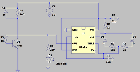
The traditional resistor ladder for the astable mode of the 555 timer isn't PWM-friendly. Though the duty cycle changes with changing resistance values, the frequency of the wave also changes and neither of these changes scale linearly. I had to add a diode network outside of the 555 to account for this.
For user experience purposes, I decided to use a digital potentiometer from Dan Julio that uses capacitive touch as an input. The capacitive touch exists as a region on which one can slide their finger to adjust the digital potentiometer's output.


The 555 timer's output leads to an NPN BJT, which ultimately controls the state of the fan's motor. I included a flyback diode to deal with inductive flyback voltages from switching action.
I concatenated all of these into a single circuit, yielding the system diagram to the right.

I spiced the captured schematic and obtained the waveforms below. Varying the values of the resistor ladder mimicking the digital potentiometer resulted in the expected change in duty cycle but not frequency.

PCB Design
As we were required to design 2-layer boards for the purpose of lowering lead times, I used the top layer of my board almost exclusively for a ground plane. This made for easy routing of many component lead holes and a low-impedance ground path. I also included test points for +12V and GND
You’ll notice that all components that can only be soldered from the bottom layer (screw terminals, JST connector) are routed completely on the bottom layer. In case I had to mill the PCB in-house, the vias would not be plated through. This is OK for a TH resistor, as one can solder both lead sides, but not for a JST connector. I learned that the hard way when working on my Hot-Swap Imager Adapter.

A render of the full PCB includes a quote and decal from my favorite novel, "Zen and the Art of Motorcycle Maintenance" by Robert Pirsig. The missing models are screw terminals, which I would use to connect to peripherals and to my 12VDC ACDC converter, which I purchased from a 3rd party vendor.

Top

Bottom
Enclosure Design
I designed two separate assemblies that would be connected only electrically; one was the fan assembly and the other housed my custom PCB, TUI, and all other circuitry.
The enclosure for the circuitry contains 4 3D-printed parts. Two of these enclose the digital potentiometer and present the capacitive touch surface to the user. The other two pieces enclose my custom PCB that is wired to the fan.
The digital potentiometer enclosure is fastened to the PCB enclosure via screws and is angled for ergonomic purposes.

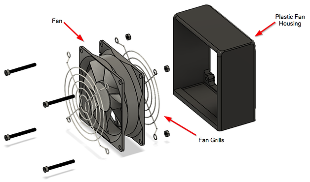
The fan assembly protects fingers with 2 fan grills and uses a ring to encapsulate the fan and keep it stable during use.
Below is an animation to conceptualize how all of these pieces fit together.