Mark Hofmeister
SIDO Buck
Converter PCB
Client
ECE 2250: Power Electronics
Location
Pittsburgh, PA
Year
2023
Resources
For my graduate-level Power Electronics class, another classmate and I were required to delve into a recent research paper in the DC-DC converter domain and do some extra analysis/simulation to probe the paper's questions a little bit deeper. I decided to go even further and implement the proposed DC-DC converter topology on a custom PCB and measure its true effectiveness. The report (in the resources section) details some additional simulation data and the full results of our testing. You can read it if you'd like, but it's dull as can be. I'd like to describe a bit more of my PCB design process below.
BOM
Design Files
Report
Report Appendices

Proposed Topology
Multiple-output DC-DC converter technology is gaining popularity in applications requiring multiple regulated DC output terminals. For example, electric vehicle power distribution networks and telecommunication networks require precisely regulated DC sources of multiple outputs, often from a single source [2]. The problem is that multiple-output systems introduce more complex topologies that introduce novel challenges in the design and implementation of such systems. Specifically, multi-stage control systems and highly non-linear characteristics arise. A group from Xi'an Jiaotong University suggested a single-inductor, dual-output (SIDO) converter topology [1] and did a bunch of fancy math and simulation to analyze the harmonics/nonlinearities arising from such a circuit:

S1 and S2 are tied together in a complementary fashion - i.e., when S1 is on, S2 is off, and vice versa. R1 and R2 represent 2 separate loads. S0 operates on a separate control scheme from S1 and S2.
The control system for this SIDO design consists of 2 control stages; the first stage controls S1 and S2 by reading the voltage across output 1 and using it to split the power between the 2 outputs.


The second stage controls S0 by reading the voltage across output 2 and using it to regulate the amount of power transferred into the entire second stage of the system.
Therefore, control stage 1 directly keeps the power to output 1 constant, and control stage 2 controls how much total power is going into the system based on the voltage across output 2.
topology implementation: schematic
I mimicked the topology of the paper's proposed topology as closely as possible. I placed footprints for potentiometers on the load in the case that I wanted to see the effect of changing the load impedance.

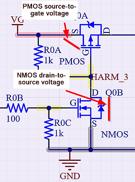
The paper [1] shows the use of an NMOS as a high-side switching element at multiple points of the circuit. To achieve high-side switching with ground as a low signal voltage reference, I implemented the converter’s switching functionality by using an NMOS-controlled-PMOS topology. This allows the use of active-high switching logic on an NMOS that controls a PMOS acting as a high-side switch, making possible the use of low control voltages to drive high source voltages. It also makes my life easier when programming everything as active high.
My design includes pull-up resistors between the PMOS gate and source and pull-down resistors between the NMOS gate and ground to prevent spurious switching.

In addition, the current through a capacitor is given by:

Without an included discrete series resistance, the FET gate’s capacitance may have a very low equivalent series resistance. Therefore, I put a series resistor on the gate of the NMOS to limit large current draw at the onset of a fast-rising edge through the MOSFET’s gate capacitance.

The complicated control scheme aims to keep steady output power/voltages amid input voltage swings. I'm using a constant input voltage, so I don't need any of that circuitry, but I'm still keeping the control signals to the two outputs inverted. Therefore, I added an inverter in between the gates of the subcircuits 1 and 2.
This required an extra inverter IC and LDO to power said IC:

I nicely separated the circuits in the schematic sheet and color-coded nets of note.
Component Selection
Though the components used are quite simple in theory, component selection for this board was tricky. I had to pay extra attention to power, current, and voltage ratings on all components, as this is most certainly the highest-power board I've made.
For example, I usually don't care about the series resistance on an inductor, unless I want a higher resistance on a ferrite bead to suppress its Q factor and therefore resonant noise spikes. However, I had to be careful to pick an inductor that can handle lots of current and not burn up from heat losses.
I also had to be very careful with the MOSFETs. In particular, I needed FETs that could handle some serious current and were in packages like TO-220 that integrate heat dissipation capacity.
I also needed to make sure that they could handle the necessary voltages at all points of the FET. When the PMOS gate is pulled to ground, the source-to-drain voltage is effectively equal to the input voltage supplied to the board, which can be as high as 30V. This same criterion applies to the drain-to-source voltage that the NMOS must handle when it is in cutoff region.


I chose 5W potentiometers, but ended up pushing upwards of 25W through them and they only slightly began to smoke.
topology implementation: PCB
While the pcb layout usually looks very different from the schematic, I kept this layout very similar to the order of the schematic. This is a circuit in which I like to see the generalized power flow concretized in copper. You can see test headers to power the circuit and inject control signals and test points to measure output voltages and harmonics at multiple nodes.
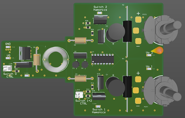
Front

Back
I was restricted to 1 oz. copper for this design, but I was liberal as can be with wide, polygonal traces. Not only am I avoiding burning up my board, I'm also trying to minimize the parasitic resistances and inductances in the traces to approach the ideal as closely as possible.

Top

Bottom
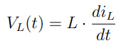
I usually pay extra attention to low inductance on power delivery lines that involve quick-switching digital ICs, but the concept is just as important in switching power supplies. Any power supply line will have parasitic inductance, and the voltage across an inductor is given by:

Therefore, rapid current changes caused by switching result in a considerable voltage drop of the power supply parasitics, sagging the power supply line considerably. This is (in part) remedied by the capacitor on the buck converter output, which acts as a local charge source to filter out high-frequency switching harmonics. However, I tried to eliminate this inductance from the start because I had the space to do it and this board needs to be close to ideal.
test results
I was curious about the transients on the different nodes of the PMOS for each output. I knew that the drain node tied to the output would be filtered by the big capacitor, but the gate and source nodes are independent of this (neglecting intinsic parasitic capacitances between the 3 terminals.)

The load node, as expected, had negligible harmonics and a relatively steady output. However, very large voltage spikes can be seen in many of the time-domain waveforms captured by the oscilloscope, concentrated at the PMOS gate and source nodes, and peak in our measurements when S1 is driven with an 80% duty cycle and S0 is driven with a 50% duty cycle. The maximum observed transient spikes are almost quadruple that of the 15VDC input voltage.

PMOS 1 Gate node at S0 = 50% D.C., S1 = 80% D.C., peak spike = 55.2V

PMOS 1 Source node at S0 = 50% D.C., S1 = 80% D.C., peak spike = 43.6V
These spikes occur at the moment that the NMOS switches off, therefore dropping the PMOS into cutof region. As discussed above, the voltage across an inductor is given by:
As current cannot instantaneously change in an inductor, these voltage transients should be expected during periods of fast switching where the inductor resists rapid changes in current via increases in voltage, which appear here at the PMOS gate and source nodes. These transients do not occur in our abstract circuit analysis because we assume ideal state transitions between switches 1 and 2. We seem to be observing latency between the complimentary switching of switch 1 and switch 2, which might be attributed to the selected inverter, CD4049UBE, which is shown to have a maximum latency of 120ns. It may also arise from die mismatch of the discrete transistors used in subcircuits 1 and 2.
If this SIDO buck converter topology is to be utilized effectively, components must be selected to withstand both the steady state voltage, current, and power conditions and the transient voltage and current spikes. Furthermore, switching elements that are matched in the same silicon die and a low-latency inverter might decrease switching transient severity, as will using high switching duty cycles to decrease the peak transient value.
Furthermore, one expects that the square waves used to drive the transistors would result in odd-integer multiple harmonics of the fundamental square wave frequency (20 kHz,) as these square waves have a duty cycle given by

While we do see integer multiple harmonics that are evenly spaced on the spectrum, we see spectral components at all integer multiple frequencies of the fundamental, not just odd integer multiples. We also do not see constant 1/n scaling of the amplitudes of the harmonic spikes. For example, the below spectra show harmonics at integer multiple frequencies, but with an amplitude pattern closer to that of an absolute-valued sinc function. If this SIDO buck converter topology is to be utilized effectively, this harmonic content must be taken into account when analyzing efficiencies. Specifically, if high switching frequencies are used, care must be taken to select switching elements that will minimize harmonic losses.


PMOS 1 Gate node at S0 = 50% D.C., S1 = 80% D.C., spectrum 20kHz - 820kHz
PMOS 1 Source node at S0 = 50% D.C., S1 = 80% D.C., spectrum 20kHz - 820kHz
References
[1] H. Zhang et al., 2020, Multiple-Harmonic Modeling and Analysis of Single-Inductor Dual-Output Buck DC–DC Converters. , IEEE Journal of Emerging and Selected Topics in Power Electronics, Volume 8, Issue 4, pages 3260 - 3271.
S. Litran et al., 2022, Multiple-Output DC-DC Converters: Applications and Solutions.
R. Erickson, D. Maksimovic, 2020, ”Fundamentals of Power Electronics, Third Edition.”
Y. Wang et al., 2017, Effect of Circuit Parameters on the Stability and Boundaries of Peak Current Mode Single-Inductor Dual-Output Buck Converters, IEEE Transactions on Industrial Electronics, Volume 65, Issue 7, pages 5445 - 5455.
A. El Aroudi et al., 2015, A Review on Stability Analysis Methods for Switching Mode Power Converters, IEEE Journal on Emerging and Selected Topics in Circuits and Systems, Volume 5, Issue 3, pages 302–315.
W. Xu et al., 2009, A Dual-Mode Single-Inductor Dual-Output Switching Converter With Small Ripple, IEEE Transactions on Power Electronics, Volume 25, Issue 3, pages 614 - 623.